BEWARE: This project has been deprecated since the arrival of the pic0rick project in 2024
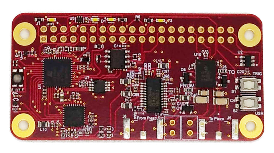
the up5k lit3rick open hardware ultrasound pulse echo board
What’s the hardware?
- FPGA: Lattice UP5K. Onboard RAM for 64k points saves.
- Onboard flash : W25X10CLSNIG
- Pulser : HV7361GA-G: can manageg up to +-100V pulses. Onboard is 5V pulse.
- AD8331 for gain - ~40dB gain.
- ADC: AD9629BCPZ-65: 12bits, reaching 64Msps here
- DAC: MCP4812-E/MS for 8us gain segments
Content
- Hardware files. Stemming from the forkable upverter design.
- Utilities to program the up5k: no FTDI, all through the RPi header, using its SPI bus to program either the board flash, or the fpga directy.
- The python tools: to facilitate the acquisitions.
- The cursed gateware: for the current gateware linked to the python library.
Remarks on hardware
- R26 is to be removed if we are using two transducers or one transducer with on element. Am i right?
- To separate TX/RX, indeed that’s R26 that should be removed.
- 5V/GND: What is used for? HV +/- must be use if we want to use an external voltage supply for the pulses?
- You can put two jumpers on the two 2x1 headers, so that 5V is connected to [HV+] source, and [HV-] is on GND. HV+ can accomodate [0 : 100V], and HV- can take [-100:0V].
- I guess “From Piezzo” and “SMA RX” are the same, with just a different connection. Is that right? Same thing for “To Piezzo” and “SMA TX”?
- “ToPiezo” is indeed the TX path, FromPiezo the RXPath.
- If we are using only one transducer for both TX and RX, how do we have to connect it?
- By default, the TX and RX SMAs are connected (with R26, a 0R). So you can only put in place one SMA an connect this piezo to this SMA.
Some images, unipolar pulse at Vpulse = 5V
Python setup
An example from the py_fpga folder, summarized. Check the visualisation of the acquisitions below.
# Setting the fpga buses
fpga = py_fpga(i2c_bus=i2c_bus, py_audio=p, spi_bus=spi)

# Setting the
fpga.set_waveform(pdelay=1, PHV_time=11, PnHV_time=1, PDamp_time=100)

# Setting the gain values
hiloVal = 1 # High or low.
dacVal = 250 # on a range from 0 to 512
fpga.set_HILO(hiloVal)
fpga.set_dac(dacVal)

# Setting the VGA
startVal,nPtsDAC = 250, 16
for i in range(nPtsDAC):
	fpga.set_dac(int(startVal + (i*(455-startVal))/nPtsDAC), mem=i)

# Reading 10 successive acquisitions
dataI2S = fpga.read_fft_through_i2s(10)

# Getting the detailed buffer (8192pts at 64msps)
dataSPI = fpga.read_signal_through_spi()

# "Manually" calculating the FFT and reading it
fpga.calc_fft()
time.sleep(3/1000.0) # normally takes ~800us to compute 8192pts
dataFFT = fpga.read_fft_through_spi()
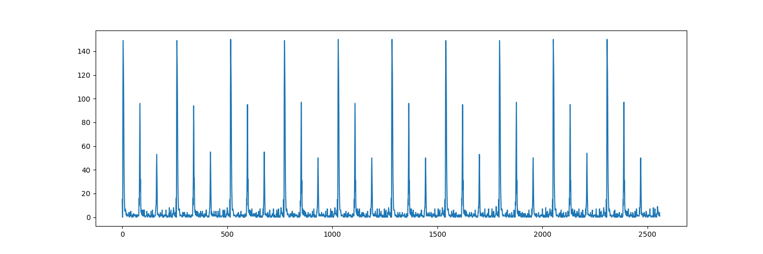
Content of the dataI2S
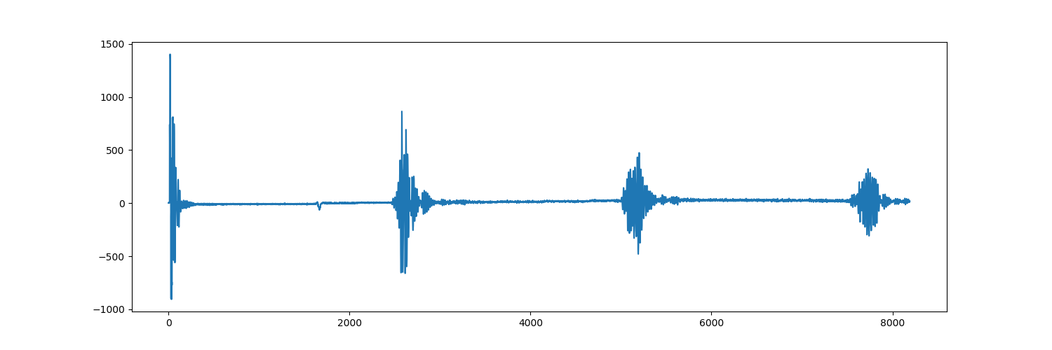
Content of the dataSPI
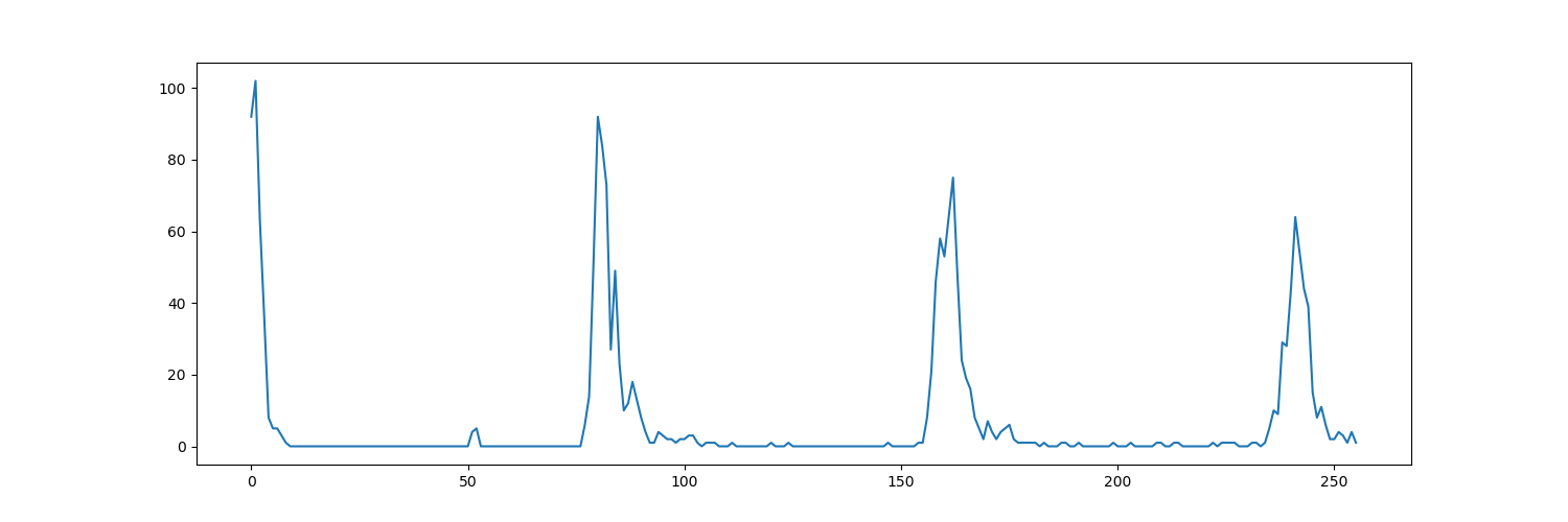
Content of the dataFFT
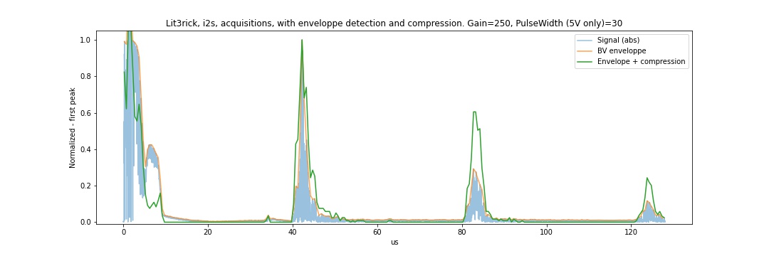
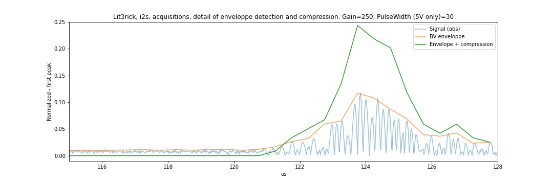
Efficiency of enveloppe extraction and compression
Benchmarking
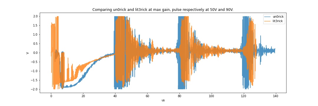
Benchmarking against the un0rick board
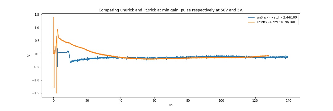
Checking the level of noise in each board, at max gain (no transducer plugged).
Changelog / TODO
- v1.1ca (not released)
- Put in AD8332
- Add external clock
- Expose gain pad
- Think of a FTDI+HV daughter board
- v1.0 initial release
- 12bits ADC
- AD8331
- i2s connections, along with i2c and spi, + uart (on buttons)
- TODO: still some finetuning with i2s streaming (slight offset over long period)
License
This work is based on two previous TAPR projects, the echOmods project, and the un0rick project - its boards are open hardware and software, developped with open-source elements as much as possible.
Copyright Kelu124 (kelu124@gmail.com) 2020.
- The hardware is licensed under TAPR Open Hardware License (www.tapr.org/OHL)
- The software components are free software: you can redistribute it and/or modify it under the terms of the GNU General Public License as published by the Free Software Foundation, either version 3 of the License, or (at your option) any later version.
- The documentation is licensed under a Creative Commons Attribution-ShareAlike 3.0 Unported License.
Disclaimer
This project is distributed WITHOUT ANY EXPRESS OR IMPLIED WARRANTY, INCLUDING OF MERCHANTABILITY, SATISFACTORY QUALITY AND FITNESS FOR A PARTICULAR PURPOSE.